TSMC Initiates Commercial Production of 2nm Chips at Key Taiwan Facilities
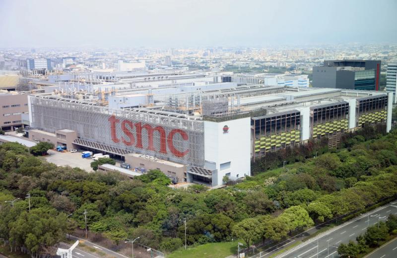
Taiwan Semiconductor Manufacturing Company (TSMC) officially commenced high-volume manufacturing of its 2-nanometer process technology today, marking a critical shift from FinFET to Gate-All-Around (GAA) transistor architecture. The announcement was made during a ceremony at the Baoshan Phase 2 facility in the Hsinchu Science Park, attended by CEO C.C. Wei and senior government officials. This milestone places TSMC roughly three months ahead of its original mass production schedule, which had been targeted for early 2026.
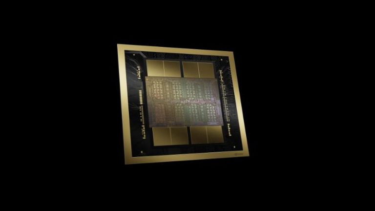
The new N2 node utilizes nanosheet transistor technology, which allows for greater control over current flow and significantly reduces power leakage compared to previous generations. According to technical specifications released by TSMC, the N2 process delivers a 10% to 15% speed improvement at the same power, or a 25% to 30% power reduction at the same speed, when compared to the N3E technology currently used in the latest smartphone chipsets. The transition to GAAFET architecture is widely considered the most complex manufacturing overhaul in the foundry’s history.
Production has simultaneously ramped up at the company’s newest fab in Kaohsiung, mirroring the output at the primary Hsinchu site. This dual-site launch strategy aims to stabilize yields quickly and meet the immediate demand from primary clients, most notably Apple and Nvidia. Industry analysts predict that the first consumer devices utilizing these 2nm chips, likely the A20 application processor for Apple’s 2026 iPhone lineup, will enter the packaging phase by the second quarter of next year.
The economic scale of this deployment is massive, with the total investment in the 2nm ecosystem estimated at over $65 billion spread across multiple expansion phases. Local officials in Hsinchu noted that the Baoshan plant has secured new dedicated water recycling infrastructure to handle the increased resource intensity of extreme ultraviolet (EUV) lithography at this density. The facility is expected to reach a monthly capacity of 30,000 wafers by the end of the first quarter of 2026.
This development exerts significant pressure on competitors Samsung Electronics and Intel Foundry, both of which are aggressively pursuing their own next-generation nodes. While Intel has claimed its 18A process is technically equivalent to 2nm, TSMC’s ability to reach volume production with verified yields in late 2025 solidifies its dominance in the high-performance computing sector. TSMC shares rose 2.4% on the Taiwan Stock Exchange following the confirmation of the early production start.