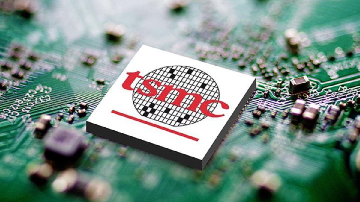
TSMC Begins Risk Production on 1.4 nm A14 Process Node
TSMC successfully produces the first functional chips on its A14 (1.4 nm-class) process at Fab 20 in Hsinchu, achieving yields of 68 percent on a 256 Mb SRAM test vehicle. The milestone arrives nine months ahead of the original roadmap and positions the foundry to capture orders for Apple’s A20 and M6 processors in late 2027. Risk production wafers incorporate gate-all-around nanosheet transistors and backside power delivery for the first time in volume manufacturing.
A14 delivers 28 percent higher transistor density than the upcoming N2 (2 nm) node, reaching 980 million transistors per square millimeter in high-performance libraries. Power efficiency improves by 42 percent at iso-performance versus N3E, with logic scaling of 1.18× over N2P through EUV double-patterning on critical metal layers. The node introduces cobalt inner vias and ruthenium outer interconnects, reducing resistance by 35 percent at M0-M3 levels.
Apple reserved 85 percent of initial A14 capacity under a $28 billion multi-year agreement signed in October. The deal guarantees 120,000 wafers monthly starting Q4 2027 at $32,000 per wafer, a 60 percent premium over N3E pricing. Nvidia and AMD secure the remaining slots for next-generation Instinct and Zen 6 dies, with Broadcom allocating 8 percent for custom AI silicon.
TSMC invests $42 billion in Fab 20 Phase 2, installing 28 ASML High-NA EUV scanners priced at €400 million each. The facility operates at full ramp will output 180,000 A14 wafers per month by 2029, consuming 4.8 gigawatts of power supplied through dedicated offshore wind contracts. Construction crews completed cleanroom certification December 10, enabling first tool move-in last week.
Early test chips demonstrate 5.8 GHz all-core boost on a 120-core Arm design at 1.1 volts, consuming 285 watts total package power. Leakage current drops 55 percent versus N2 through super-high-κ dielectrics and optimized nanosheet channel width. Backside power rails reduce IR drop by 18 percent, enabling 12 percent higher frequency uplift in GPU shaders during internal Apple benchmarks.
The node introduces carbon-nanotube interconnect pilots on select metal layers, cutting resistivity 40 percent versus copper at 8 nm pitch. TSMC confirms full cobalt fill at contact level, eliminating tungsten barriers that limited N3 scaling. High-NA lithography achieves 8 nm resolution with 0.55 numerical aperture, supporting sub-14 nm metal pitches without quadruple patterning.
Competitor Intel delays its 14 Å (1.4 nm equivalent) process to 2028 after repeated gate-all-around yield issues at the Oregon D1X fab. Samsung cancels its 1.4 nm roadmap entirely, redirecting resources to 2 nm production starting mid-2026. The gap widens TSMC’s advanced-node market share to 69 percent through 2029, per VLSI Research projections.
Apple’s A20 SoC, taped out on A14 last month, integrates 240 billion transistors across a 480 mm² die. Early silicon validates 48 TOPS NPU performance at 18 watts and 40 percent graphics uplift versus M4 Max. Mass production ramps in September 2027 for iPhone 20 and MacBook Pro 2028 models.
TSMC shares rise 8 percent in Taipei trading, pushing market capitalization above $1.1 trillion. Analysts raise 2028 revenue guidance to $182 billion on A14 pricing power. The company begins customer tape-outs next quarter, with design rule manuals distributed under NDA to 42 partners including Qualcomm, MediaTek, and Google Tensor teams.
The breakthrough solidifies Taiwan’s chokehold on sub-2 nm manufacturing, prompting U.S. Commerce Department officials to fast-track $12 billion in CHIPS Act subsidies for TSMC Arizona’s delayed 2 nm fab. Risk production success triggers contractual bonuses worth $3.8 billion from Apple, payable upon 70 percent yield certification scheduled for March 2026.
A14 marks the final node before TSMC’s planned transition to angstrom-era naming with A10 (1.0 nm) in 2029. The company confirms ribbonFET transistors and direct backside contacting will debut on that process, targeting 1.3 trillion transistors per chip in high-end configurations. The advance keeps Moore’s Law alive for at least another half-decade in commercial silicon.