ASML’s New EUV Light Source Advance Promises Up to 50 Percent More Chip Production
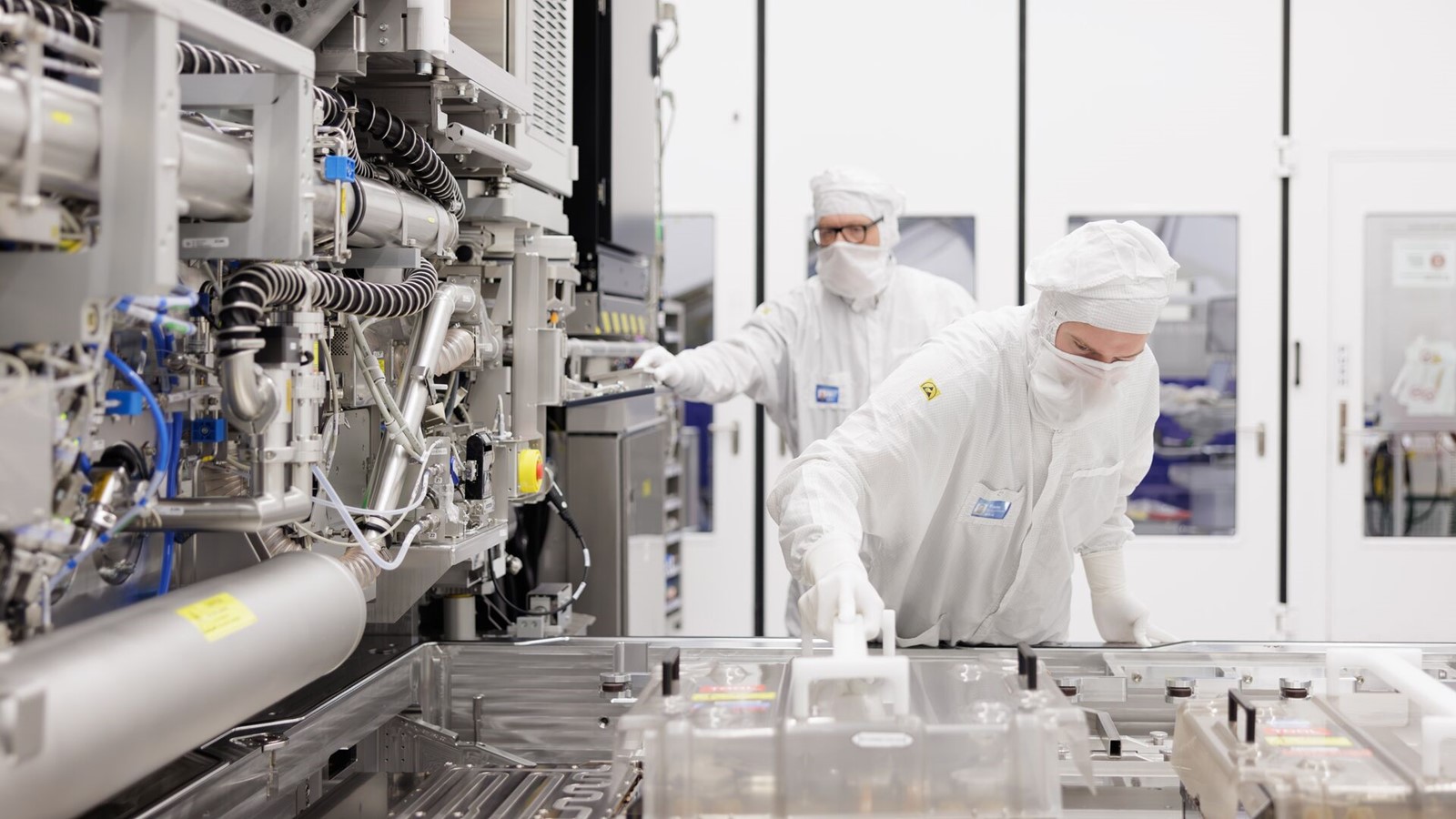
ASML Holding has revealed a significant breakthrough in its extreme ultraviolet lithography technology that could transform semiconductor manufacturing. Researchers at the company have developed a way to increase the power of the EUV light source from the current 600 watts to 1,000 watts. This enhancement allows machines to expose silicon wafers more quickly, directly boosting the number of chips produced per hour. The advancement helps maintain ASML’s leading position in the industry as the sole provider of commercial EUV systems used by major chipmakers. It addresses growing demand for advanced chips while keeping costs in check.
The core of this technology involves generating EUV light at a 13.5-nanometer wavelength. Machines fire a carbon dioxide laser at tiny droplets of molten tin to create plasma hotter than the surface of the Sun. This plasma emits the precise light needed to pattern circuits on wafers coated with photoresist. The new method doubles the rate of tin droplets to around 100,000 per second and uses additional laser pulses to shape the plasma more efficiently. These changes improve energy conversion and deliver higher usable power without major redesigns to existing equipment.
By reaching 1,000 watts, the systems can reduce exposure times during the lithography process. Current EUV machines process about 220 silicon wafers per hour. With this upgrade, that figure could climb to around 330 wafers per hour by the end of the decade. Since each wafer holds dozens or even thousands of individual chips depending on their size, the overall output rise translates to up to 50 percent more chips from the same machines. This efficiency gain lowers production costs per chip and helps fabs meet surging needs for processors in artificial intelligence, smartphones, and other devices.
ASML’s lead technologist for EUV source light, Michael Purvis, emphasized the reliability of the achievement during an interview at the company’s facilities near San Diego. He described it as a stable system capable of delivering 1,000 watts under real-world customer conditions rather than a brief demonstration. The company has already mapped out pathways to even higher levels like 1,500 watts or potentially 2,000 watts in the future. Such progress strengthens ASML’s defenses against emerging competition from the United States and China in advanced lithography tools.
This development arrives at a time when chipmakers face intense pressure to scale production rapidly. Higher throughput on existing EUV platforms means factories can expand capacity without proportional increases in floor space, energy use, or new machine purchases. It supports continued innovation in smaller, more powerful semiconductors that power modern computing. The timeline points to meaningful implementation by the end of the decade, aligning with long-term industry roadmaps.
What do you think this breakthrough could mean for the future of chip availability and pricing, share your thoughts in the comments.